Wafer Cleaning Equipment Market Size, Share, Trends, Growth, and Industry Analysis, By Technology (Cryogenic Aerosols, Super-Critical Fluid Cleaning Process, Wet Chemical Cleaning, Vapour Dry Cleaning, and Aqueous Cleaning Process), By Equipment (Single Wafer Spray, Batch Spray Cleaning System, Scrubber, Single Wafer Cryogenic, and Batch Immersion Cleaning System), By Size (<150mm, 200mm and 300mm), By Application (CIS memory, RFID device, MEMS, LED Interposer and Others), By Operational Mode (Semi-automated, Manual, and Automated), Regional Analysis and Forecast 2032.
Wafer Cleaning Equipment Market Trend
Global Wafer Cleaning Equipment Market size was USD 9.26 billion in 2023 and the market is projected to touch USD 16.92 billion by 2032, at a CAGR of 7.83% during the forecast period.
Cleaning of wafers is essential since it provides scrubbing away of the contaminants and residues from the surface of the wafer. It, therefore, ensures that the production of high quality semiconductors is evident. Impurities inside the semiconductor can very easily determine its performance level, hence making effective cleaning methods a necessary feature for manufacturers.
Increased demand over the last several years has characterized the need for wafer cleaning equipment due to advanced semiconductor devices that find use in several applications, such as consumer electronics, automotive systems, and telecommunications. Technology advancements and artificial intelligence, Internet of Things, and 5G networks drive this boom in the market. Hence, key players in the industry are now resorting to new cleaning solutions based on innovative efficiency, cost minimization, and environmental reduction. The demand for such miniaturized and high-performance equipment is increasing with the semiconductor manufacturing process; thus, this kind of equipment will contribute towards the steady growth of the market and offer further growth opportunities for its manufacturers and suppliers.
Wafer Cleaning Equipment Report Scope and Segmentation.
Report Attribute |
Details |
Estimated Market Value (2023) |
USD 9.26 Billion |
Projected Market Value (2032) |
USD 16.92 Billion |
Base Year |
2023 |
Historical Year |
2018-2022 |
Forecast Years |
2024 – 2032 |
Scope of the Report |
Historical and Forecast Trends, Industry Drivers and Constraints, Historical and Forecast Market Analysis by Segment- Based on By Technology, By Equipment, By Size, By Application, By Operational Mode, & Region. |
Segments Covered |
By Technology, By Equipment, By Size, By Application, By Operational Mode, & By Region. |
Forecast Units |
Value (USD Million or Billion), and Volume (Units) |
Quantitative Units |
Revenue in USD million/billion and CAGR from 2024 to 2032. |
Regions Covered |
North America, Europe, Asia Pacific, Latin America, and Middle East & Africa. |
Countries Covered |
U.S., Canada, Mexico, U.K., Germany, France, Italy, Spain, China, India, Japan, South Korea, Brazil, Argentina, GCC Countries, and South Africa, among others. |
Report Coverage |
Market growth drivers, restraints, opportunities, Porter’s five forces analysis, PEST analysis, value chain analysis, regulatory landscape, market attractiveness analysis by segments and region, company market share analysis. |
Delivery Format |
Delivered as an attached PDF and Excel through email, according to the purchase option. |
Dynamic Insights
The major driver behind the market is growing demand for semiconductor devices with increasing technological advancement and spreading electronic applications in automotive, healthcare, and consumer electronics. With increasing complexity in the semiconductor manufacturing processes, the requirement of effective and clean cleaning agents becomes absolutely critical for ensuring high yield and performance.
On the other hand, the market also brings about challenges: high costs associated with advanced cleaning equipment and an urgent need to innovate through continuous improvement in line with innovations in technologically rapid changes. Moreover, environmental regulations in respect to chemicals used in the cleaning process may sometimes limit the manufacturers' freedom. However, opportunities lie with businesses that put more money into Research and Development, thereby enabling development of clean technologies and methods for cleaning that not only embrace the environment but are also in conformity with the set regulations of the nation while responding to these industrial demands.
Drivers Insights
The increased need for semiconductor devices is because the adoption rate of cutting-edge technologies like artificial intelligence and the Internet of Things along with 5G telecommunications technologies is high. These need high-performance chips and also require very clean wafer cleaning processes. In the process, increased complexities are found in chips, and hence wafer cleaning becomes of utmost importance. Clean solutions ensure that semiconductors are intact with respect to their performance by removing all contaminants and residues. This trend is forcing the manufacturers to invest in high sophisticated wafer cleaning equipment, which thus triggers market growth.
Continuous innovation in cleaning technologies is a significant driver of the wafer cleaning equipment market. Companies are developing advanced cleaning processes, such as dry cleaning and plasma cleaning, which enhance efficiency while minimizing damage to delicate wafers. These new methods reduce downtime and improve production yields, making them attractive to manufacturers. Additionally, automation and smart technologies are being integrated into cleaning systems, providing real-time monitoring and control, further optimizing the cleaning process. As manufacturers seek to improve productivity and reduce costs, the demand for cutting-edge wafer cleaning equipment is likely to increase.
Restraints Insights
The initial investment required for advanced wafer cleaning equipment can be substantial, posing a challenge for manufacturers, especially smaller firms. High costs are associated with the purchase, installation, and maintenance of sophisticated cleaning systems. This financial burden can deter companies from upgrading their equipment, leading to reliance on outdated cleaning technologies that may not meet modern standards. As a result, this restraint can limit market growth and hinder the adoption of more efficient and effective cleaning solutions.
Increasing regulations regarding the use of hazardous chemicals in cleaning processes can restrict manufacturers' options for cleaning solutions. Regulatory bodies are imposing stricter guidelines to minimize environmental impact, which can complicate the formulation and application of cleaning agents. Manufacturers must invest in research and development to create eco-friendly alternatives that comply with regulations, adding to operational costs and potentially delaying product releases. This regulatory landscape can act as a barrier to market growth.
Opportunities Insights
With the rising global emphasis on sustainability, there is a growing opportunity for manufacturers to develop eco-friendly wafer cleaning technologies. Solutions that reduce water usage, minimize chemical waste, and utilize non-toxic cleaning agents can meet both regulatory requirements and market demand for greener practices. Companies that prioritize sustainability in their product offerings can gain a competitive edge and appeal to environmentally conscious consumers and manufacturers. This shift towards sustainable practices not only enhances brand reputation but also aligns with global trends toward corporate responsibility and environmental stewardship.
Segment Analysis
The wafer cleaning equipment market is classified by technology, which includes diverse techniques with the goal of maximizing the cleaning of semiconductor wafers. Cryogenic aerosols use very low temperatures to clean up the wafers without leaving residues behind. This leads to highly efficient removal of contamination and retention of the integrity of the wafer. The super-critical fluid cleaning process employs super-critical fluids, possibly carbon dioxide, to dissolve and remove particles and residues from the wafer surface. It is an environmentally friendly alternative to using traditional solvents. Wet chemical cleaning remains highly applied in the removal of contaminants by liquid chemicals, which are introduced into wafers either by immersion or spraying. Vapor dry cleaning uses vaporized solvents, on the other hand, to clean without liquids, thus reducing the risk of damaging the wafer. Lastly, aqueous cleaning applies water-based solutions to clean and is supposed to be friendly for the environment. All these technologies are applicable in the semiconductor manufacturing of specific needs in the requirement of very high quality in their products.
In equipment terms, the wafer cleaning market involves different systems designed for various cleaning processes. More precisely, the specific process in single wafer spray systems is dedicated to cleaning individual wafers, meaning that it prevents interference with other wafers during the cleaning process. In contrast, a batch spray cleaning system can accommodate several wafers at once and uses more production-oriented environments to account for time and volume as factors. Scrubber systems provide a robust cleaning application that establishes mechanical and chemical action on the surface of the wafer to eliminate stubborn dirt. Single wafer cryogenic equipment uses cryogenic technology for point-source cleaning, thereby suited for sensitive wafers that require gentle handling. Lastly, the batch immersion cleaning system provides a robust cleaning methodology since it entails placing multiple wafers inside a cleaning solution and therefore provides full coverage and comprehensive cleaning. This diversity has freed semiconductor manufacturers to choose their appropriate cleaning solution that they feel is relevant to their production needs and specifications for wafer.
The market is also divided by wafer size, including <150mm, 200mm, and 300mm. The <150mm segment primarily consists of older technology and smaller devices that are mostly still in demand for niche applications and specialized uses. The 200mm wafer size is relatively widespread in the mass production of a wide range of semiconductor devices, including integrated circuits and sensors, which makes this segment significant for most manufacturers. This new semiconductor technology, on the 300mm wafers, enables both more powerful and more efficient devices while at the same time optimizing manufacturing processes. As industries continue to pursue larger wafers for greater performance and cost savings, the need for size-specific cleaning solutions increases, driving innovations in both cleaning equipment and technologies themselves.
The application segment of the wafer cleaning equipment market includes various specialized uses, such as CIS memory, RFID devices, MEMS, and LED interposers. CIS memory (Contact Image Sensor) applications require meticulous cleaning to ensure the highest image quality and device performance, necessitating advanced cleaning technologies. RFID devices (Radio-Frequency Identification) also demand rigorous cleaning to eliminate contaminants that could affect signal transmission and device reliability. The MEMS (Micro-Electro-Mechanical Systems) segment requires precision cleaning methods to ensure the functionality and performance of tiny components, which are sensitive to contamination. Lastly, LED interposers, used in advanced lighting and display applications, necessitate cleaning solutions that maintain the integrity and performance of the delicate structures involved.
Regional Analysis
In North America, the market is fuelled by the presence of major semiconductor manufacturers and ongoing investments in research and development. The U.S. stands out as a leading player, benefiting from cutting-edge technology and a robust semiconductor ecosystem. Europe follows closely, with countries like Germany and France showing growth due to increased demand for electronics and automotive applications, along with supportive government initiatives promoting semiconductor production.
In Asia-Pacific, the market dominates globally, driven by the presence of leading semiconductor foundries in countries such as China, Taiwan, South Korea, and Japan. These nations are investing heavily in advanced semiconductor production facilities, propelling demand for wafer cleaning equipment. China’s initiatives to become self-reliant in semiconductor manufacturing are a significant growth driver. Japan and South Korea are also leading contributors, with established electronics industries fostering high demand for advanced wafer cleaning technologies.
Competitive Landscape
Leading players in the industry are Applied Materials, Lam Research, and Tokyo Electron, who have experience spanning over decades, complete product lines, and strong relationships with their customers and whom invest heavily in developing their latest versions of cleaning technologies to meet the changing needs in semiconductor manufacturing. Suppliers with solid supply chains and global presence can capitalize on growing demands for semiconductor devices across applications.
In addition to these leaders, a number of niche players start to surface, focused on specific technologies or regional markets. Companies, like ChemTrace, KMG Chemicals, and Ultratech are gaining scale by offering something unique about their cleaning solutions that uniquely caters to some segments of the wafer cleaning market, such as use of ecofriendly cleaning agents or advanced mechanical cleaning systems. The modern cleaning equipment is actually gaining more ground for competition because of the trend toward automation and smart manufacturing, with companies that need to move their facilities toward powerful technology.
Additionally, strategic partnerships, collaborations, and acquisitions are some of the other prevailing measures observed within major players that help them better their position in the market as well as enhance their product portfolio. In general, these collaborations give way to high-tech cleaning solutions adhering strictly to industry standards.
List of Key Players:
Global Wafer Cleaning Equipment Report Segmentation:
ATTRIBUTE |
DETAILS |
By Technology |
|
By Equipment |
|
By Size |
|
By Application |
|
By Geography |
|
Customization Scope |
|
Pricing |
|
Objectives of the Study
The objectives of the study are summarized in 5 stages. They are as mentioned below:
Research Methodology
Our research methodology has always been the key differentiating reason which sets us apart in comparison from the competing organizations in the industry. Our organization believes in consistency along with quality and establishing a new level with every new report we generate; our methods are acclaimed and the data/information inside the report is coveted. Our research methodology involves a combination of primary and secondary research methods. Data procurement is one of the most extensive stages in our research process. Our organization helps in assisting the clients to find the opportunities by examining the market across the globe coupled with providing economic statistics for each and every region. The reports generated and published are based on primary & secondary research. In secondary research, we gather data for global Market through white papers, case studies, blogs, reference customers, news, articles, press releases, white papers, and research studies. We also have our paid data applications which includes hoovers, Bloomberg business week, Avention, and others.
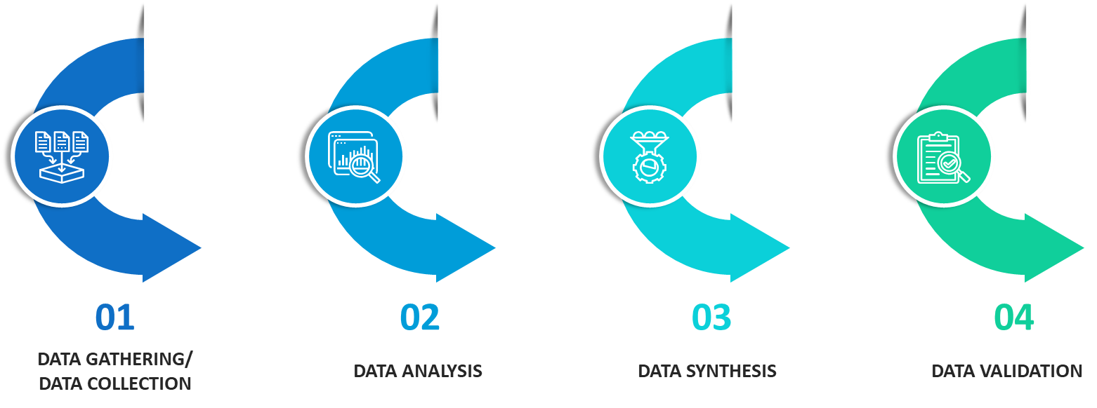
Data Collection
Data collection is the process of gathering, measuring, and analyzing accurate and relevant data from a variety of sources to analyze market and forecast trends. Raw market data is obtained on a broad front. Data is continuously extracted and filtered to ensure only validated and authenticated sources are considered. Data is mined from a varied host of sources including secondary and primary sources.
Primary Research
After the secondary research process, we initiate the primary research phase in which we interact with companies operating within the market space. We interact with related industries to understand the factors that can drive or hamper a market. Exhaustive primary interviews are conducted. Various sources from both the supply and demand sides are interviewed to obtain qualitative and quantitative information for a report which includes suppliers, product providers, domain experts, CEOs, vice presidents, marketing & sales directors, Type & innovation directors, and related key executives from various key companies to ensure a holistic and unbiased picture of the market.
Secondary Research
A secondary research process is conducted to identify and collect information useful for the extensive, technical, market-oriented, and comprehensive study of the market. Secondary sources include published market studies, competitive information, white papers, analyst reports, government agencies, industry and trade associations, media sources, chambers of commerce, newsletters, trade publications, magazines, Bloomberg BusinessWeek, Factiva, D&B, annual reports, company house documents, investor presentations, articles, journals, blogs, and SEC filings of companies, newspapers, and so on. We have assigned weights to these parameters and quantified their market impacts using the weighted average analysis to derive the expected market growth rate.
Top-Down Approach & Bottom-Up Approach
In the top – down approach, the Global Batteries for Solar Energy Storage Market was further divided into various segments on the basis of the percentage share of each segment. This approach helped in arriving at the market size of each segment globally. The segments market size was further broken down in the regional market size of each segment and sub-segments. The sub-segments were further broken down to country level market. The market size arrived using this approach was then crosschecked with the market size arrived by using bottom-up approach.
In the bottom-up approach, we arrived at the country market size by identifying the revenues and market shares of the key market players. The country market sizes then were added up to arrive at regional market size of the decorated apparel, which eventually added up to arrive at global market size.
This is one of the most reliable methods as the information is directly obtained from the key players in the market and is based on the primary interviews from the key opinion leaders associated with the firms considered in the research. Furthermore, the data obtained from the company sources and the primary respondents was validated through secondary sources including government publications and Bloomberg.
Market Analysis & size Estimation
Post the data mining stage, we gather our findings and analyze them, filtering out relevant insights. These are evaluated across research teams and industry experts. All this data is collected and evaluated by our analysts. The key players in the industry or markets are identified through extensive primary and secondary research. All percentage share splits, and breakdowns have been determined using secondary sources and verified through primary sources. The market size, in terms of value and volume, is determined through primary and secondary research processes, and forecasting models including the time series model, econometric model, judgmental forecasting model, the Delphi method, among Flywheel Energy Storage. Gathered information for market analysis, competitive landscape, growth trends, product development, and pricing trends is fed into the model and analyzed simultaneously.
Quality Checking & Final Review
The analysis done by the research team is further reviewed to check for the accuracy of the data provided to ensure the clients’ requirements. This approach provides essential checks and balances which facilitate the production of quality data. This Type of revision was done in two phases for the authenticity of the data and negligible errors in the report. After quality checking, the report is reviewed to look after the presentation, Type and to recheck if all the requirements of the clients were addressed.